A wafer is a thin slice of semiconductor material, typically made of silicon, that serves as the substrate for the fabrication of integrated circuits in the field of VLSI. During the fabrication process, the wafer undergoes a series of processes such as doping, lithography, etching, and deposition to create the desired patterns and structures for the integrated circuits. After the integrated circuits have been fabricated on the wafer, they are then separated and packaged into individual chips for use in various electronic devices. The quality and uniformity of the wafer can greatly impact the performance and reliability of the integrated circuits fabricated on it.
The above paragraph provides a summarized brief on Wafer in VLSI. To gain more understanding of Wafer, please read the rest of the article.
The usage of wafers in the VLSI industry has been crucial for the growth and development of the electronics industry. Wafers are the basic building blocks for creating integrated circuits (ICs), which are used in a wide range of electronic devices, including smartphones, computers, and consumer electronics. The demand for wafers has increased as the demand for consumer electronics continues to grow.
Wafer Size and Preparation Method
Wafers are thin, flat disks usually made of silicon and come in a variety of sizes. Wafers used in VLSI fabrication are typically between 100 and 300 millimeters in diameter and between 0.5 and 1 millimeter thick. The most common size used in the industry is 300mm, although smaller sizes, such as 200mm and 150mm are still used in some applications.
The wafers are produced by slicing a cylindrical boule of semiconducting material into thin disks using a specialized saw. Once the wafer has been sliced, it is subjected to a series of process steps, including deposition and pattering of various materials, etching away unwanted materials, and lithography to create the desired microchips. The resulting chips are then tested and packaged for use in various electronic devices.
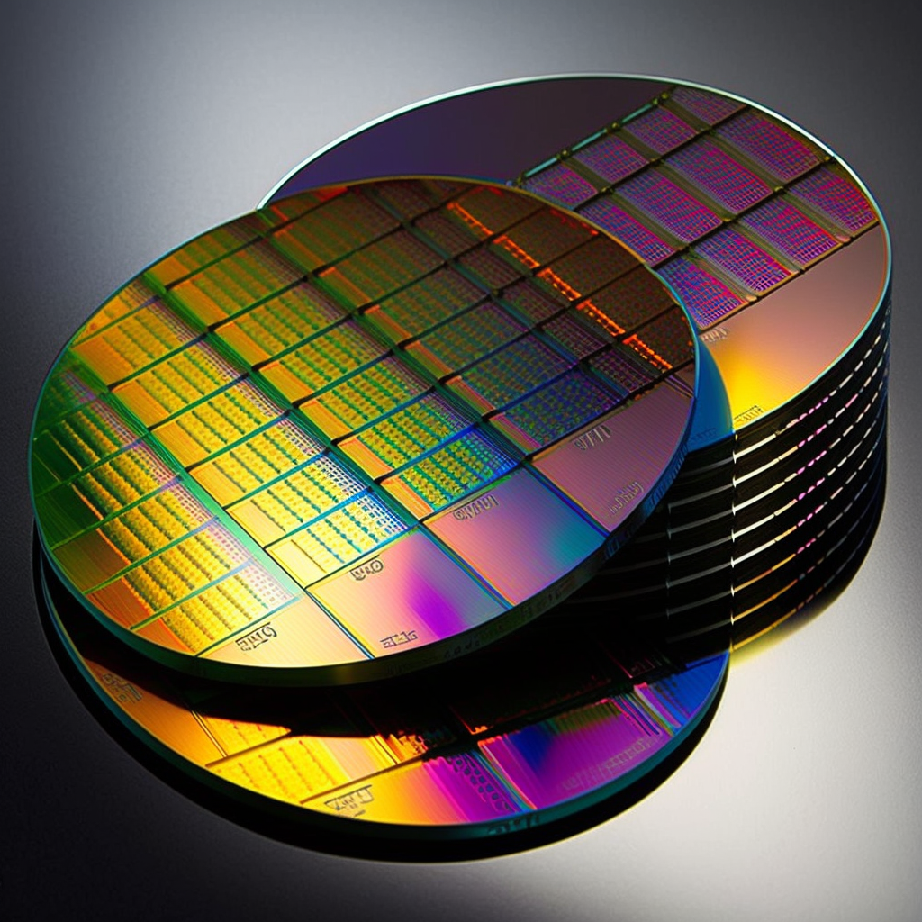
Silicon wafers
Use of Wafers in VLSI Industry
The use of wafers in VLSI technology provides several advantages, including increased efficiency and reduced costs. By fabricating multiple chips on a single wafer, the cost per chip can be significantly reduced, as many of the process steps can be performed in a single batch. Additionally, the use of wafers allows for increased efficiency in the manufacturing process, as multiple chips can be processed in parallel.
In conclusion, the wafer is an essential component in the fabrication of microchips and integrated circuits in the field of VLSI. Its use provides significant advantages, including increased efficiency and reduced costs, making it an important aspect of modern electronics manufacturing.
Discover more from VLSIFacts
Subscribe to get the latest posts sent to your email.
Dear Sir or Madam:
I’m Helen from WEISS in China,I am writing this mail to build up a business relationship with you about silicon wafer.
We offer different diameters IC Grade silicon wafer from 25.4mm to 300mm in cost-effective and stable quality. And we accept customized wafer enquiry.
We carry a wide selection of Prime Standard CZ and FZ Ingots in stock at all times.
We supply:
1. Standard CZ silicon wafer, /, N and P type, 0.001-100 ohm-cm, SSP/DSP;
2. Customize CZ silicon wafer, any thickness, super thick or supper thin, thickness from 100um to 3000um.
3. Standard FZ silicon wafer, /, N and P type or intrinsic, 1,000 to 2,000 ohm-cm, SSP/DSP;
4. Customize FZ silicon wafer, Intrinsic, Resistivity> 20,000 ohm-cm.
Could you please kindly send RFQs to me if necessary? Thank you!