For the design of any circuit with the CMOS technology; We need parallel or series connections of nMOS and pMOS with a nMOS source tied directly or indirectly to ground and a pMOS source tied directly or indirectly to Vdd. A basic CMOS structure of any 2-input logic gate can be drawn as follows:

2 Input NAND Gate
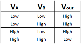
TRUTH TABLE
 CIRCUIT

The above drawn circuit is a 2-input CMOS NAND gate. Now let’s understand how this circuit will behave like a NAND gate. The circuit output should follow the same pattern as in the truth table for different input combinations.
Case-1 : VA – Low & VB – Low
As VA and VB both are low, both the pMOS will be ON and both the nMOS will be OFF. So the output Vout will get two paths through two ON pMOS to get connected with Vdd. The output will be charged to the Vdd level. The output line will not get any path to the GND as both the nMOS are off. So, there is no path through which the output line can discharge. The output line will maintain the voltage level at Vdd; so, High.
Case-2 : VA – Low & VB – High
VA – Low: pMOS1 – ON; nMOS1 – OFF
VB – High: pMOS2 – OFF; nMOS2 – ON
pMOS1 and pMOS2 are in parallel. Though pMOS2 is OFF, still the output line will get a path through pMOS1 to get connected with Vdd. nMOS1 and nMOS2 are in series. As nMOS1 is OFF, so Vout will not be able to find a path to GND to get discharged. This in turn results the Vout to be maintained at the level of Vdd; so, High.
Case-3 : VA – High & VB – Low
VA – High: pMOS1 – OFF; nMOS1 – ON
VB – Low: pMOS2 – ON; nMOS2 – OFF
The explanation is similar as case-2. Vout level will be High.
Case-4 : VA – High & VB – High
VA – High: pMOS1 – OFF; nMOS1 – ON
VB – High: pMOS2 – OFF; nMOS2 – ON
In this case, both the pMOS are OFF. So, Vout will not find any path to get connected with Vdd. As both the nMOS are ON, the series connected nMOS will create a path from Vout to GND. Since, the path to ground is established, Vout will be discharged; so, Low.
In all the 4 cases we have observed that Vout is following the exact pattern as in the truth table for the corresponding input combination.
2 Input NOR Gate
TRUTH TABLE
 CIRCUIT

The above drawn circuit is a 2-input CMOS NOR gate. Now let’s understand how this circuit will behave like a NOR gate.
Case-1 : VA – Low & VB – Low
VA – Low: pMOS1 – ON; nMOS1 – OFF
VB – Low: pMOS2 – ON; nMOS2 – OFF
Path establishes from Vdd to Vout through the series connected ON pMOS transistors and Vout gets charged to Vdd level. No path from Vout to GND. Therefore, no discharging and hence Vout will be High.
Case-2 : VA – Low & VB – High
VA – Low: pMOS1 – ON; nMOS1 – OFF
VB – High: pMOS2 – OFF; nMOS2 – ON
In this case path establishes from Vout to GND through nMOS2, but no path to Vdd. So, Vout would get discharged and will be at level Low.
Case-3 : VA – High & VB – Low
VA – High: pMOS1 – OFF; nMOS1 – ON
VB – Low: pMOS2 – ON; nMOS2 – OFF
The explanation is similar as case-2. Vout will be at level Low.
Case-4 : VA – High & VB – High
VA – High: pMOS1 – OFF; nMOS1 – ON
VB – High: pMOS2 – OFF; nMOS2 – ON
No path to Vdd. Path establishes from Vout to GND. So, Vout will be at level Low.
In all the 4 cases we have observed that Vout is following the expected value as in 2 input NOR gate truth table.
For the design of ‘n’ input NAND or NOR gate:
Let’s say n = 3
In case of NAND gate, 3 pMOS will be connected in parallel and 3 nMOS will be connected in series, and other way around in case of 3 input NOR gate. The same pattern will continue even if for more than 3 inputs.
Tech Tip : Move your essential Circuit design & simulator software into the cloud with hosted citrix xendesktop at an affordable citrix xendesktop cost and experience the ease of comfort to remotely access it from anywhere on any device. If you run a small business then try out QuickBooks Enterprise Hosting and Office 365 Enterprise E3 suite from Apps4Rent.
Very helpful!
Thank you
Excellent ease.of.understand
Thank you Deep
excellent
Thanks Pavani
Thank you so much.
it was very helpful.
Most Welcome Ali.
thanks alot
Thank you, this was so easy to understand.
Thank you!
Most Welcome
thanku
Most Welcome