The semiconductor industry is constantly evolving, driven by the relentless demand for higher performance, lower power consumption, and faster time-to-market. One of the most exciting trends reshaping chip development today is chiplet based design. But what exactly is a chiplet based design, and why is it gaining so much attention? In this blog post, we’ll explore the concept of chiplets, their benefits, challenges, and how they are transforming the future of semiconductor innovation.
What is a Chiplet Based Design?
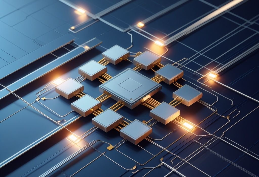
A chiplet based design breaks down a large, complex integrated circuit into multiple smaller, modular chips called chiplets. Instead of fabricating one massive monolithic chip, designers create these smaller chiplets separately and then integrate them within a single package using advanced packaging technologies.
Imagine building a high-performance computer from different specialized components like CPU cores, memory blocks, and I/O interfaces – each manufactured independently but seamlessly connected. This modular approach offers greater flexibility, better yields, and faster innovation.
Why Use Chiplet Based Design?
1. Better Manufacturing Yield and Lower Cost
Large monolithic chips have a higher chance of defects, which can drastically reduce manufacturing yield and increase cost. By splitting the design into smaller chiplets, each can be tested and manufactured independently, improving overall yield and reducing wastage.
2. Accelerated Development and Time-to-Market
Chiplet design allows reuse of existing, proven IP blocks. Designers can mix and match chiplets from different vendors or previous projects, speeding up development and reducing risk.
3. Heterogeneous Integration
Chiplets enable integration of different technologies – such as logic, memory, analog, and RF components – that may be fabricated on different process nodes. This is challenging in traditional monolithic designs but becomes feasible and efficient with chiplets.
4. Scalability and Customization
Chiplet architectures allow designers to scale performance by adding or upgrading individual chiplets without redesigning the entire chip. This flexibility supports diverse application needs and customization.
How Do Chiplets Connect?
Chiplets communicate through advanced packaging solutions such as:
- Silicon Interposers: Thin silicon layers with dense wiring that connect chiplets with high bandwidth.
- Embedded Multi-die Interconnect Bridge (EMIB): A small silicon bridge embedded in the package substrate to link chiplets.
- Advanced Fan-Out (AFO) Packaging: Uses redistribution layers to route signals between chiplets on the package.
These methods ensure fast, power-efficient communication between chiplets, mimicking on-chip interconnect speeds.
Examples of Chiplet Based Design
AMD Ryzen and EPYC Processors
AMD’s Ryzen and EPYC CPUs are among the most prominent examples of chiplet based design in commercial products. Instead of building a large monolithic CPU, AMD uses multiple smaller CPU core chiplets connected via a high-speed interconnect called Infinity Fabric. This approach has allowed AMD to scale core counts efficiently, improve yields, and reduce costs, enabling competitive performance against monolithic designs.
Intel’s Foveros Technology
Intel’s Foveros is an advanced 3D packaging technology that stacks chiplets vertically. It allows integration of logic chiplets fabricated on different process nodes with memory chiplets in a compact package. This technology is used in Intel’s Lakefield processors, combining high-performance cores with low-power cores and memory in a single package.
Challenges in Chiplet Based Design
While chiplets offer many advantages, they also introduce new challenges:
- Standardization: The industry is still working on universal standards for chiplet interfaces to ease integration.
- Testing Complexity: Testing individual chiplets and the final integrated package requires sophisticated methodologies.
- Thermal Management: Efficiently dissipating heat across multiple chiplets is critical for reliability.
- Design Partitioning: Deciding how to split functionality across chiplets needs careful architectural planning.
Chiplet based design is revolutionizing semiconductor development by enabling modular, scalable, and cost-effective chip architectures. Real-world successes from AMD, Intel, and NVIDIA demonstrate how chiplets unlock new possibilities in performance and efficiency. As packaging and interface standards mature, chiplet designs will become even more prevalent, shaping the future of electronics.
Discover more from VLSIFacts
Subscribe to get the latest posts sent to your email.