Skip to content

VLSIFacts

Let's Program the Transistors

  • Home
  • DHD
    • Digital Electronics
    • Fault Tolerant System Design
    • TLM
    • Verification
    • Verilog
    • VHDL
    • Xilinx
  • Embedded System
    • 8085 uP
    • 8086 uP
    • 8051 uC
  • VLSI Technology
    • Analog Electronics
    • Memory Devices
    • VLSI Circuits
  • Interview
    • Interview Experience
    • Training Experience
    • Question Bank
  • Notifications
  • QUIZ
  • Community
  • Job Board
  • Contact Us

Circuit Design of a Sequence Detector

Posted on February 4, 2016June 17, 2025 By vlsifacts 3 Comments on Circuit Design of a Sequence Detector

This post illustrates the circuit design of Sequence Detector for the pattern “1101”. State Machine diagram for the same Sequence Detector has been shown below. Click here to realize how we reach to the following state transition diagram.

Mealy machine of 1101 Sequence Detector
Mealy machine of “1101” Sequence Detector

Click here to learn the step by step procedure of “How to synthesize a state machine / How to boil down a state machine to the circuit level”.

Now as we have the state machine with us, the next step is to encode the states. For 4 states:

State     Encoding

S0            00

S1            01

S2            10

S3            11

We need only 2 flipflops to represent these 4 states. For this example we will be using T Flipflips to design the circuit.

Let’s draw the state transition table using the Excitation table of T flipflop

PS

Q2(t)  Q1(t)

X

Input

NS

Q2(t+1) Q1(t+1)

Excite (T)

T2  T1

O

Output

   0        0   0 0           0   0   0    0
   0        0   1 0           1   0   1    0
   0        1   0 1           0   1   1    0
   0        1   1 0           1   0   0    0
   1        0   0 0           0   1   0    0
   1        0   1 1           1   0   1    0
   1        1   0 1           0   0   1    0
   1        1   1 0           1   1   0    1

Now to realize the combinational logic we have to find out the Boolean expression for 3 output variables (of the above table) T2, T1 and O in terms of 3 input variable Q2(t), Q1(t) and X.

T2T1
T2 for Sequence Detector
T1 for Sequence Detector
YBoolean Expressions
Y for Sequence Detector
T2 = Q2′(t)Q1(t)X’ + Q2(t)Q1′(t)X’ +

        Q2(t)Q1(t)X

T1 = Q1(t)X’ + Q1′(t)X = Q1(t) ⊕ X

O = Q2(t)Q1(t)X

Let’s draw the respective circuit diagram for the given Sequence Detector.

Circuit diagram of synthesized Sequence Detector

Spread the Word

  • Click to share on Facebook (Opens in new window) Facebook
  • Click to share on X (Opens in new window) X
  • Click to share on LinkedIn (Opens in new window) LinkedIn
  • Click to share on Pinterest (Opens in new window) Pinterest
  • Click to share on Tumblr (Opens in new window) Tumblr
  • Click to share on Pocket (Opens in new window) Pocket
  • Click to share on Reddit (Opens in new window) Reddit
  • Click to email a link to a friend (Opens in new window) Email
  • Click to print (Opens in new window) Print

Like this:

Like Loading...

Related posts:

  1. State Machine Diagram for Pattern Recognition / Sequence Detector
  2. Mealy Vs. Moore Machine
  3. Mealy to Moore and Moore to Mealy Transformation
  4. Circuit Design of Parity Generator
DHD, Digital Electronics Tags:Circuit Design of State Machine, FSM, FSM Design, Mealy Machine Design, Pattern Matching, Sequence Detector

Post navigation

Previous Post: State Machine Diagram for Pattern Recognition / Sequence Detector
Next Post: State Machine Diagram for Parity Generator

Comments (3) on “Circuit Design of a Sequence Detector”

  1. chitra barvekar says:
    September 22, 2017 at 8:30 pm

    can you please explain the asynchronous sequence detector or any finite state machine

    Reply
  2. babu says:
    February 26, 2018 at 5:48 pm

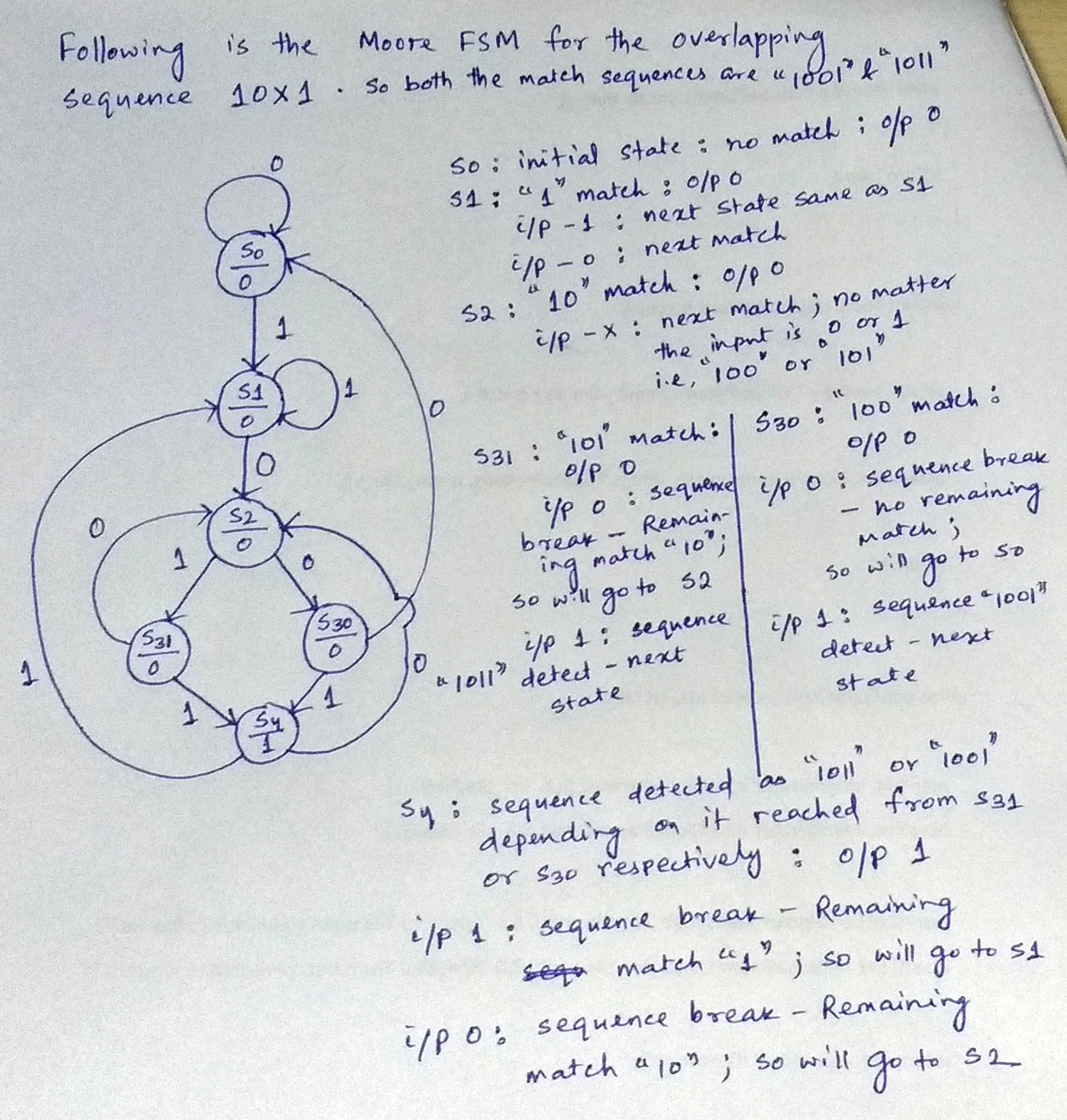
    can you please draw moore FSM overlapping for 10X1 sequence detection

    Reply
    1. Sidhartha says:
      March 7, 2018 at 2:24 pm

      Dear Babu,

      Sorry for replying you so late. Hope you must have resolved the problem. But for your reference and for the reference of the other readers we are posting the solution of your query. In the following figure I have drawn the FSM with the detection of bit from MSB towards LSB, whereas in the above published post the detection is done from LSB to MSB.

      Reply

Leave a Reply Cancel reply

Your email address will not be published. Required fields are marked *

Top Posts & Pages

  • ASCII Code
  • Circuit Design of a 4-bit Binary Counter Using D Flip-flops
  • NAND and NOR gate using CMOS Technology
  • Binary to Gray Code Conversion and Vice Versa
  • AND and OR gate using CMOS Technology

Copyright © 2025 VLSIFacts.

Powered by PressBook WordPress theme

Subscribe to Our Newsletter

%d