Problem Statement:
Design a circuit for an edge triggered 4-bit binary up counter (0000 to 1111). When it reaches “1111”, it should revert back to “0000” after the next edge. Use positive edge triggered D flip-flop (shown in the below figure) to design the circuit.
| Pin | Input / Output | Description |
| D | Input | Data Input |
| CLK | Input | Clock Input |
| Q<3:0> | Output (4-bits) | Count Output |

Solution:
The flip flop to be used here to design the binary counter is D-FF.
Let’s draw the excitation table for the D-FF
| Present State (Q) | Input (D) | Next State (Q+) |
| 0 | 0 | 0 |
| 0 | 1 | 1 |
| 1 | 0 | 0 |
| 1 | 1 | 1 |
The characteristic equation for the D-FF is: Q+ = D
We need to design a 4 bit up counter. So, we need 4 D-FFs to achieve the same.
Let’s draw the state diagram of the 4-bit up counter

Let’s construct the truth table for the 4-bit up counter using D-FF
| Present State
(Q3 Q2 Q1 Q0) | Next State
(Q3+ Q2+ Q1+ Q0+) | D3 | D2 | D1 | D0 |
| 0000 | 0001 | 0 | 0 | 0 | 1 |
| 0001 | 0010 | 0 | 0 | 1 | 0 |
| 0010 | 0011 | 0 | 0 | 1 | 1 |
| 0011 | 0100 | 0 | 1 | 0 | 0 |
| 0100 | 0101 | 0 | 1 | 0 | 1 |
| 0101 | 0110 | 0 | 1 | 1 | 0 |
| 0110 | 0111 | 0 | 1 | 1 | 1 |
| 0111 | 1000 | 1 | 0 | 0 | 0 |
| 1000 | 1001 | 1 | 0 | 0 | 1 |
| 1001 | 1010 | 1 | 0 | 1 | 0 |
| 1010 | 1011 | 1 | 0 | 1 | 1 |
| 1011 | 1100 | 1 | 1 | 0 | 0 |
| 1100 | 1101 | 1 | 1 | 0 | 1 |
| 1101 | 1110 | 1 | 1 | 1 | 0 |
| 1110 | 1111 | 1 | 1 | 1 | 1 |
| 1111 | 0000 | 0 | 0 | 0 | 0 |
Now constructing the K-Maps and finding out the logic expressions for D3, D2, D1, D0
| D3 | D2 |
 |  |
| D3 = Q3Q2′ + Q3Q0′ + Q3Q1′ + Q3’Q2Q1Q0 | D2 = Q2Q0′ + Q2Q1′ + Q2’Q1Q0 |
| D1 | D0 |
 |  |
| D1 = Q1’Q0 + Q1Q0′ = Q1 ⊕ Q0 | D0 = Q0′ |
So, we found the value of D3, D2, D1, D0 in terms of Q3, Q2, Q1, Q0.
Let’s draw the designed circuit of the 4-bit up counter using D-FF
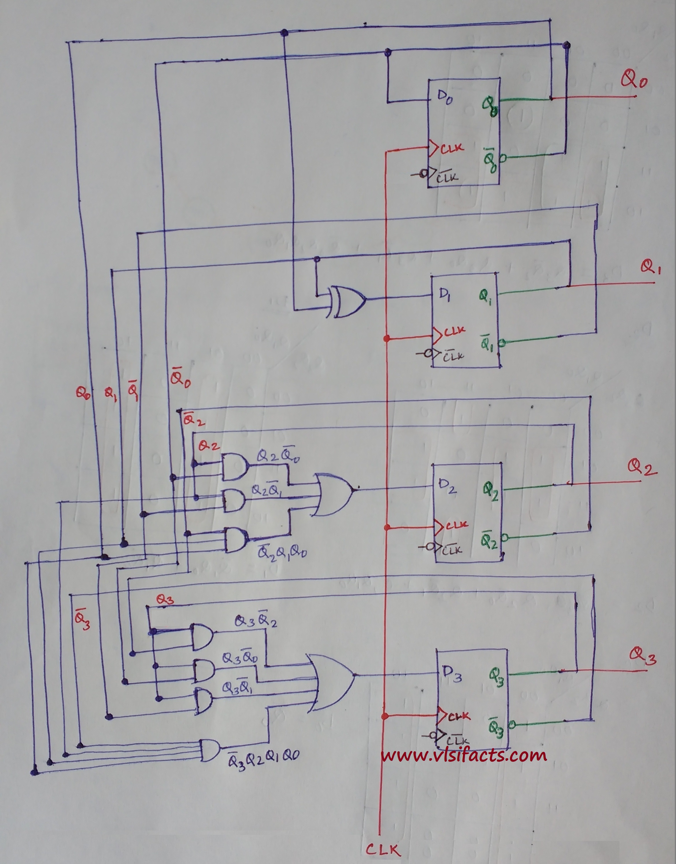
The counter output would be collected from Q3, Q2, Q1 and Q0.
Discover more from VLSIFacts
Subscribe to get the latest posts sent to your email.
hello , i m really very impressed to you .
can u please post or send me the synthesis of FSM.
Hey Deepak,
Thanks for the appreciation. We would definitely publish a post on the synthesis of the FSM very soon.
really very glad to see ur smart work.It helped me a lot baiyaa..tank u soo much
Hey Aruna,
Thanks a lot. Keep visiting VLSIFacts. Lot more to come. Subscribe to the blog and like our FB page.
Nice explanation. Keep it up
Hey Ritesh,
Thanks for your appreciation. Stay tuned to VLSIFacts for more such posts.
Nice sir
Thanks a lot
hi Mr Siddharth
ho design a 4 bit ripple counter
Hi Sunitha,
Sure, I would upload the same this week.
You get a much nicer equivalent circuit if you notice that
D2 = Q2 ⊕ (Q1Q0)
D3 = Q3 ⊕ (Q2Q1Q0)
It should not be the case that the number of gates you need to add with each new flip flop increases.
thank you sir
Welcome Nathan
1: Use several jk flip-flops to realize a counter. the counting sequence is from 0000 through 1011, and then go back to 0000. please draw the circuit.
2: How can you solve the question 1 if you only have D flip flops? only explain it.
Hi Mehdi,
Sorry for such a late reply. I would create separate posts for these designs and would upload.
Hey
First of all i would like to thank you for making this.
I have a question tho.
Is this acording the MOORE method and if yes would it mean that for a 3 bit counter i would jus have to remove the q3/d3.
And would it be possible to add a function to make it count like 1 3 5 1 3 5…..
Hi,
First of all I am very sorry for such a delayed comment. And thank you very much for your appreciation.
Now to your questions:
(i) Yes it is according to MOORE method.
(ii) For a 3 bit counter, of course you would need 3 Flip-flops only. But it’s not like that you will only remove the 3rd FF. We have to think about the input logic as well. Yes you can remove D3 and Q3 from the truth table then go through the whole process we have done for the 4 bit counter.
(iii) to make it count like 1 3 5 1 3 5….. adding a function to the existing design would also work but that is a tricky and one. Again why would you go for a 4 bit counter if your largest count is 5. So, it is better to start the process of design from the beginning and design the circuit.
Let me know if you have any further doubt.
I want to convert Q0 Q1 Q2 Q3 decimal numbers and want to display on 7 segment display. Please guide me.
You are required to design a 4-bit even up-counter using D flip flop by converting combinational circuit to sequential circuit. The counter will only consider even inputs and the sequence of inputs will be 0-2-4-6-8-10-0.
You are required to perform following tasks:
1. Draw the State diagram.
2. Generate State & Transition Table.
3. Generate simplified Boolean Expression.
4. Design the final Circuit diagram.
PLEASE SOLVE THIS
THANK YOU SO MUCH. IT HELPED ME ALOT
Most welcome Adarsh
First of all i am very great full to you sir.
My question is that how can i design this circuit on PC soft form?
This is my Semester end project of DLD.
I want some information like you can please help me in guiding what software i use for designing this circuit in soft form.